PIN Diode
The PIN diode or p-i-n diode has an additional layer of intrinsic material between the p-type and n-type layers that gives it some useful characteristics.
PIN Diode Tutorial Includes:
PIN Diode basics
PIN Diode characteristics & specifications
Other diodes: Diode types
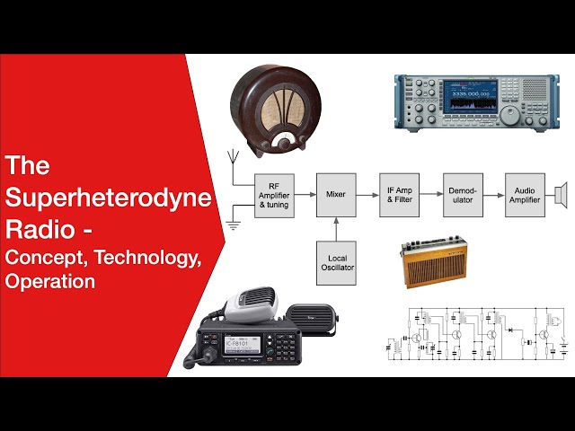
Although diodes with a basic PN junction are by far the most popular type of diode in use, other types of diode may be used in a number of applications. One type that is used for a variety of circuits is the PIN diode. This form of diode is used in a number of areas. The PIN diode is very good for RF switching, and the PIN structure is also very useful in photodiodes.
The PIN diode found its first applications in 1952 as a low frequency high power rectifier. It was also used in a number of microwave applications, although it took until around 1960 before its use became more popular in this application. A further use of the PIN diode is as a photo-detector (photodetector or photo-diode) where its structure is particularly suited to absorbing light.
PIN diode structure
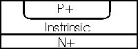
The PIN diode receives its name from the fact that is has three main layers. Rather than just having a P type and an N type layer, the PIN diode has three layers:
- P-type layer
- Intrinsic layer
- N-type layer
The instrinic layer of the PIN diode is the one that provides the change in properties when compared to a normal PN junction diode. The intrinsic region comprises of the undoped, or virtually undoped semiconductor, and in most PIN diodes it is very thin - of the order of between 10 and 200 microns.
There are a two main structures that can be used, but the one which is referred to as a planar structure is shown in the diagram. In the diagram, the intrinsic layer is shown much larger than if it were drawn to scale. This has been done to better show the overall structure of the PIN diode.
PIN diodes are widely made of silicon, and this was the semiconductor material that was used exclusively until the 1980s when gallium arsenide started to be used.
PIN diode characteristics
The intrinsic layer between the P-type and N-type regions of the PIN diode enable it to provide properties such as a high reverse breakdown voltage, and a low level of capacitance, and there are also other properties such as carrier storage when it is forward biased that enable it to be used for certain microwave applications.
It is found that at low levels of reverse bias the depletion layer become fully depleted. Once fully depleted the PIN diode capacitance is independent of the level of bias because there is little net charge in the intrinsic layer. However the level of capacitance is typically lower than other forms of diode and this means that any leakage of RF signals across the diode is lower.
When the PIN diode is forward biased both types of current carrier are injected into the intrinsic layer where they combine. It is this process that enables the current to flow across the layer.
The particularly useful aspect of the PIN diode occurs when it is used with high frequency signals, the diode appears as a resistor rather than a non linear device, and it produces no rectification or distortion. Its resistance is governed by the DC bias applied. In this way it is possible to use the device as an effective RF switch or variable resistor producing far less distortion than ordinary PN junction diodes.
PIN diode uses and advantages
The PIN diode is used in a number of areas as a result of its structure proving some properties which are of particular use.
- High voltage rectifier: The PIN diode can be used as a high voltage rectifier. The intrinsic region provides a greater separation between the PN and N regions, allowing higher reverse voltages to be tolerated.
- RF switch: The PIN diode makes an ideal RF switch. The intrinsic layer between the P and N regions increases the distance between them. This also decreases the capacitance between them, thereby increasing he level of isolation when the diode is reverse biased.
- Photodetector: As the conversion of light into current takes place within the depletion region of a photdiode, increasing the depletion region by adding the intrinsic layer improves the performance by increasing he volume in which light conversion occurs.
These are three of the main applications for PIN diodes, although they can also be used in some other areas as well.
Summary
Although not as widely used as normal PN junction diodes, PIN diodes are nevertheless used in large quantities. PIN diodes are particularly used in RF applications where there low levels of capacitance and also their switching and variable resistance properties make them very good in switching and variable attenuator applications.
More Electronic Components:
Batteries
Capacitors
Connectors
Diodes
FET
Inductors
Memory types
Phototransistor
Quartz crystals
Relays
Resistors
RF connectors
Switches
Surface mount technology
Thyristor
Transformers
Transistor
Unijunction
Valves / Tubes
Return to Components menu . . .