PN Junction Diode
The PN junction diode is the most basic form of semiconductor device and its technology forms the basis of many other semiconductor devices.
Diode Tutorial Includes:
Diode types
Diode specs & ratings
PN junction diode
LED
PIN diode
Schottky barrier diode
SiC diode
Solar cell / photovoltaic diode
Varactor / varicap
Zener diode
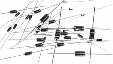
After resistors and capacitors, one of the most widely used electronic components is the PN junction diode. They are used in many different electronic circuit designs in a number of different ways.
The PN junction diode is the basic semiconductor diode format. It is used for many forms of rectification for current levels both large and small, as well as high and low voltage levels, and this semiconductor device finds many uses in all manner of electronic circuit designs.
The PN junction has the very useful property that electrons are only able to flow in one direction. As current consists of a flow of electrons, this means that current is allowed to flow only in one direction across the structure, but it is stopped from flowing in the other direction across the junction.
PN junction diodes can be obtained in a number of semiconductor materials - the earliest diodes tended to be made from germanium, but most of them today are silicon diodes.
The diode is simple in its basic concept, being formed from the junction of N-type and P-type materials, although in reality the manufacture and theory of operation are more complex.
Diode circuit symbol and polarity
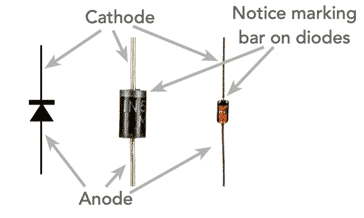
Like any diode, the PN junction diode has two connections or electrodes. This gives it its name: "di-" meaning two and "-ode" as a shortening of electrode.
One electrode of the semiconductor device is termed the anode and the other is termed the cathode. For a current to flow across the PN diode junction it must be forward biased. Under these conditions conventional current flows from the anode to the cathode, but not the other way around.
It is easy to determine the polarity of many wired diodes. The "bar" on the circuit symbol corresponds to the cathode of the diode and this is often marked by a white line around the circumference of the actual diode. Orientation for SMD diodes is less obvious and is normally determined as a result of the fact that diodes are contained in a similar package to transistors having three terminals - only two are used for the SMD diodes, but they can only be orientated in one direction.
When a PN junction diode is forward biassed, the anode is positive with resect to the cathode, and conversely, when reverse biassed the cathode is positive with respect to the anode.

This means that when a diode is used in a circuit like a rectifier, the cathode is provides the positive output - the anode still remaining more positive as shown in the circuit below.

Polarity on diode is for forward biassed / conduction condition
This circuit shows how the anode of the diode is positive with respect to cathode and the cathode is connected to the output which is positive with resect to the zero volt line. In this way the voltage polarities around the circuit are maintained.
Development of the PN junction diode
The PN junction is one of the most important structures in today's electronics scene. It forms the basis of most of today's semiconductor technology, and was the first semiconductor device to be used.
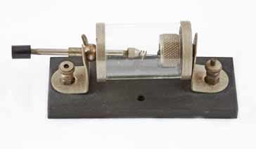
The first semiconductor diode to be used was the Cat's Whisker wireless detector used in early wireless sets. It consisted of a wire placed onto a material that was effectively a semiconductor. The point where the wire met the semiconductor then formed a small PN junction and this detected the radio signals. It was actually a form of Schottky diode, but nevertheless the earliest form of PN junction and semiconductor device.
The diode or PN junction was the first form of semiconductor device to be investigated in the early 1940s when the first real research was undertaken into semiconductor technology. It was found that small point contact diodes were able to rectify some of the microwave frequencies used in early radar systems and as a result they soon found many uses.
Today, the PN junction has undergone a significant amount of development. Many varieties of diode are in use in a variety of applications. In addition to this, the PN junction forms the basis of much of today's semiconductor technology where it is used in transistors, FETs, and many types of integrated circuit.
The PN junction is found in many semiconductor devices today including semiconductor diodes, the bipolar transistor, junction FETs, MOSFETs, diac, thyristor and the triac - it forms the basis of a huge amount of today's semiconductor technology.
Note on the PN Junction Diode Invention:
The PN junction diode was invented almsot by accident when Russell Ohl working at Bell Labs in the USA noticed some peculiarities in a sample of silicon with a crack in its structure.
Read more about Invention of PN junction diode.
PN Junction
A PN junction is typically made from a single piece of semiconductor that has two differing areas: one is made to be P-type and the other N-type.
Accordingly the different areas of the semiconductor have different properties. The N-type semiconductor has an excess of electrons whilst the P-type has an excess of holes.
The diode can be thought of consisting of the two areas being brought into intimate contact with each other.
When this occurs the holes diffuse into the N-type area and a similar process occurs for the P-type material.
When this diffusion occurs, the flow of charges sets up an electric field that starts to hinder the flow of further charge and shortly and equilibrium state is reached and no further flow of charge occurs.
Where the two areas meet and at equilibrium there are no free holes or electrons. This means that there are no available charge carries in this region. In view of the fact that this area is depleted of charge carriers it is known as the depletion region.

The depletion region is very thin - often only few thousandths of a millimetre - but this is enough to prevent current flowing in the normal way. However it is found that different effects are noticed dependent upon the way in which the voltage is applied to the junction.

Current Flow - If the voltage is applied such that the P type area becomes positive and the N type becomes negative, holes are attracted towards the negative voltage and are assisted to jump across the depletion layer.
Similarly electrons move towards the positive voltage and jump the depletion layer. Even though the holes and electrons are moving in opposite directions, they carry opposite charges and as a result they represent a current flow in the same direction.
No current flow - If the voltage is applied to the PN junction in the opposite sense no current flows. The reason for this is that the holes are attracted towards the negative potential that is applied to the P type region.
Similarly the electrons are attracted towards the positive potential which is applied to the N type region. In other words the holes and electrons are attracted away from the junction itself and the depletion region increases in width. Accordingly no current flows across the PN junction.

PN junction characteristics
While the PN junction provides an excellent rectifying action, it is not a perfect diode having infinite resistance in the reverse direction and zero resistance in the forward direction. In order that the PN junction can be used, it is necessary to know a little about its properties and characteristics with forward and reverse bias.
Looking at the characteristic plot of the PN junction, it can be seen that in the forward direction (forward biased) it can be seen that very little current flows until a certain voltage has been reached. This represents the work that is required to enable the charge carriers to cross the depletion layer. This voltage varies from one type of semiconductor to another. For germanium it is around 0.2 or 0.3 volts and for silicon it is about 0.6 volts.
It is possible to measure a voltage of about 0.6 volts across most small current diodes when they are forward biased as most of these electronic components are silicon. A small number will show a lower voltage and are likely to be germanium. Power rectifier diodes normally have a larger voltage across them but this is partly due to the fact that there is some resistance in the silicon, and partly due to the fact that higher currents are flowing and they are operating further up the curve.

In the reverse direction, a perfect diode would not allow any current to flow. In reality a small amount of current does flow, although this is likely to be very small and in the region of pico amps or microamps. It has been exaggerated on the diagram so that it can be seen. Although it is normally very low, the performance of any diode will degrade at higher temperatures and it is also found that germanium is not as good as silicon.
This reverse current results from what are called minority carriers. These are a very small number of electrons found in a P type region or holes in an N type region. Early semiconductors has relatively high levels of minority carriers, but now that the manufacture of semiconductor materials is very much better the number of minority carriers is much reduced as are the levels of reverse currents.
The basic diode PN junction is used in many electronic components throughout the whole of the electronics industry today: in many new general electronic circuit designs, RF designs and many other areas.
Even it its basic form as a diode, this electronic component is used in enormous quantities, but beyond that, the PN junction forms the bedrock of most of today's high-tech transistors, integrated circuits and other semiconductor devices. Without the PN junction, life today would be very different, and electronics would be a very different scene.
More Electronic Components:
Batteries
Capacitors
Connectors
Diodes
FET
Inductors
Memory types
Phototransistor
Quartz crystals
Relays
Resistors
RF connectors
Switches
Surface mount technology
Thyristor
Transformers
Transistor
Unijunction
Valves / Tubes
Return to Components menu . . .