
Transistor Gain: hFE, hfe & Beta, β
Current gain is one of the important electronic circuit design specifications for a bipolar transistor – three figures are often seen: Beta β, hFE & hfe, each of which is slightly different.
Transistor Tutorial Includes:
Transistor basics
Gain: Hfe, hfe & Beta
Transistor specifications
Transistor and diode numbering codes
Choosing replacement transistors
In any circuit, the current gain of a bipolar transistor will be of paramount importance. Whether the circuit is common emitter, common collector, etc, and whether it uses NPN transistors or PNP transistors.
Although other parameters of these semiconductor devices are also important, the current gain is particularly key because the bipolar transistor is a current operated device.
The transistor current gain is normally specified in terms of hFE, hfe, or the Greek letter Beta β. Although these parameters are very similar ata first glance, they are different and the right quantity should be used for the relevant elements of an electronic circuit design.
When designing any transistor circuit, it is necessary to ensure there is sufficient gain to enable the circuit to operate correctly. Gain levels can be very high for many small signal devices, with current gains up to 1000 not uncommon, but for power transistors, gains are very much lower and can sometimes be in the region of only 25 - 50.
Normally current gain specifications for transistors normally have a very wide tolerance, and therefore circuits need to be able to accommodate this. However the minimum transistor gain must be sufficient to support the correct operation of the particular circuit design.
Transistor gain & Beta, β
Bipolar transistors are what are termed current controlled devices. In other words the current flowing int he base circuit controls the level of current in the collector. Accordingly the current gain between the base and collector is the important factor in any transistor circuit design.
When undertaking many calculations in an electronic circuit design, the transistor current gain is given in terms of the Greek letter Beta; β.
This is the forward current gain for the transistor when operated in a common emitter mode. Common emitter is one of the more common circuit configurations for transistor circuit designs.

Although it is not strictly exact, the equation below is more than accurate enough for all practical calculations. This transistor gain equation is the one that is seen in most instances.
The current gain of the transistor is used not only to set up the bias conditions for the circuit design, but also to ensure that there is sufficient gain within the circuit to give the overall required function.
For example when designing a common emitter transistor circuit, the current gain figures are used to ensure that the potential divider setting the bias for the base is able to provide sufficient current.
Knowing the emitter current, it is possible to determine the base current that is needed and hence design the potential divider to provide sufficient current at the required voltage.
Transistor hfe
Transistor Hfe, hfe are often seen quoted as the current gain figure for a transistor. This can lead to some confusion, so it helps to explain what each one means.
The reason for using hfe is that it refers to way of measuring the input and output parameters of a transistor.
Z parameters are one of the basic parameters used when treating a circuit as a black box. However as a transistor exhibits a low input impedance and a high output impedance a form of parameter known as h or hybrid parameters are used.
hfe is the forward transfer characteristic, i.e. transistor gain when used in the common emitter mode.
hfe is exactly the same as the transistor Beta, β - it is just a little more correct to use it in datasheets.
DC & small signal transistor gain
The transistor gain varies slightly when measured for DC and for small signal variations.
The notations for the two figures are slightly different. Often ΒDC is used for the DC gain, and ΒAC is used for the AC gain which may also be referred to as the transistor small signal gain.
Similarly for hfe. Hfe with a capital H is used for the DC gain, where as the AC or small signal gain is denoted by hfe with a small letter h.
Transistor gain summary
There are a number of different notations that are used for transistor current gain. It is worth understanding exactly what they are and what differences exist between them.
- Beta; β: This is the basic notation for the forward current gain of a transistor and it is widely used in many electronic circuit design calculations.
- hfe: This is the current gain for a transistor expressed as an h parameter (hybrid parameter). The letter f indicates that it is a forward transfer characteristic, and the letter e indicates it is for a common emitter configuration. The small letter h indicates it is a small signal gain. hfe and small signal Beta are the same. This figure is widely used in transistor data sheets and hence within the circuit design calculations.
- hFE : The hFE parameter differs from hfe in that it is the h parameter for the DC or large signal steady state forward current gain. This figure will be used when setting up bias conditions or for use within power supply circuit designs, or other circuits where the DC gain is important.
The different abbreviation used for the transistor gain, hFE, hfe & Beta are all widely used, although the parameters Hfe, hfe tend to be more widely used in datasheets.
With the wide variation in levels of current gain found in all transistors, this makes the exact figures for current gain a little academic. Any transistor circuit design should be able to accommodate a wide variation iin the level of current gain, whether it is small signal or DC.
Points to note
There are several points which are of interest when judging the level of current gain that a transistor has:
Gain of power transistors: The gain of power transistors is typically very much less than that of small signal devices. In fact power transistors may have current gain figures of less than 50.
This lack of gain can be overcome by using another transistor to drive the power transistor, the overall current gain can be increased to the desired level. Darlington configurations where two transistors are used together may also be useful to increase the overall current gain while also retaining the high current capability of the power transistor.
Current gain varies widely: It is worth noting that for any transistor type there can be a very large spread between different devices. Normally the performance of the circuit does not depend directly on the actual current gain, especially as negative feedback is often included, or for switching applications the actual gain is not critical.
It is always wise to ensure there is enough current gain available using the minimum figure given in the datasheets.
Variation of current gain
It is normally expected that the value of current gain β for a bipolar transistor is constant, however there are some variations that occur in the value of β or hFE.
β variations with collector current: The collector current level can cause a variation in the level of β or or hFE.
- At low current: This occurs when the bipolar transistor is running at very low current levels as a result of leakage mechanisms being seen and affecting the overall transistor current. For example the specification for a BC109B operating with a collector current, IC of 10µA and a collector emitter voltage VCE of 5V has a minimum gain of 40, whereas for a collector current, IC of 2mA and a collector emitter voltage VCE of 5 V it has a minimum gain of 200.
- At high current: It is found that the level of the bipolar transistor current gain β starting to reduce as the current is increased. This results from a high level injection occurring.
Normally the bipolar transistor is biassed to operate in its linear region for analogue signals and it can be assumed that the current gain is constant. Accordingly, for good linear operation, the transistor should be operated well within its operating range and not running into the rails or drawing excessive current for the particular semiconductor device.
Temperature effects on current gain β: Temperature has a major effect on many bipolar transistor parameters, one of which is the current gain, β / hFE, etc.
Frequency: The frequency of operation will have a marked effect on the value of current gain. For low frequencies, the value of hfe, i.e. the small signal gain will not vary too much from the value for DC hFE figure - a good rule of thumb is that the mid figure for hFE can be used. As the circuit operation for any circuit should not be critically dependent upon the actual gain for the semiconductor device. If the frequency rises and even starts to approach the fT of the device, then a lower gain figure must be used.
Manufacturing spreads: As a result of the tolerances in the manufacturing processes, the current gain of bipolar transistors will vary over a considerable range. (See below).
In these descriptions the variations of β described for bipolar transistors can be equally applicable to hFE.
Datasheet specifications of current gain
As a result of the manufacturing processes, bipolar transistors typically have a wide range in their values of current gain.
As already mentioned, figures for both Hfe the DC gain and hfe the small signal AC gain. Often figures for both parameters are specified.
When giving the specification, the test conditions are outlined. The current level and collector emitter voltage are normally specified.
In view of the spread of current gain levels in these electronic components, figures for minimum, typical and maximum may be given. Often, not all of these figures are give: sometimes only the minimum figure for the current gain may be specified.
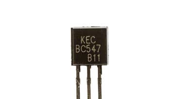
As there can be a significant variation in gain for a given type of transistor, a suffix letter on the end of the transistor part number may specify the band of gain expected for that particular device. For example a BC109B has a current gain hFE between 200 and 450, and a BC109C has a current gain hFE between 420 and 800.
Reasons for large gain differences between transistors
One of the most obvious facts about transistor parameters, is the very wide variation in the levels of gain between different transistors of the same type.
These large variations in the current gain: β hFE and hfe can occur between the same transistor type, between different batches and even different transistors manufactured ont he same wafer.
The current gain depends on manufacturing characteristics such as the thickness of the base and the doping level. These are not exactly the same from one batch to another or even one transistor to another, so the gain will vary significantly.
Looking at the structure of a planar transistor, it can be seen that the base region thickness is dependent upon the depth to which the doping for the collector region and emitter region extends. As the base region is so thin, even small variations in the depth of the doping can cause large variations in the base region thickness on top of any variations in doping of the base region.

When all these variations are summed together, these give rise to the large variation in the levels of current gain: β hFE and hfe that are seen.
Multimeter hFE measurements
Many digital multimeters, DMMs have a capacity for measuring the gain of a transistor. This can be quite a useful function, especially for checking whether a transistor is still functioning or not.
Generally this type of measurement is incorporated in the lower end digital multimeters as it is not a particularly accurate test and is generally more appropriate for hobbyist and 'quick check' style measurements of the transistor function.
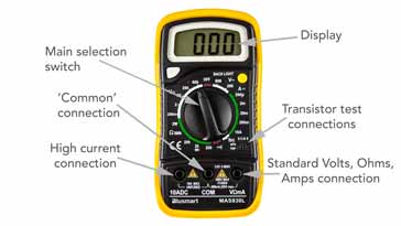
The hFE figures given within a datasheet are taken under set conditions, whereas the measurement incorporated within a digital multimeter will not be defined in the same way.
Generally the measurements made by DMMs will use DC voltages and therefore the measurement is of hFE rather than the small signal gain hfe value. Also the conditions of voltage and current for the test will not be known as these are not normally provided in the digital multimeter datasheet.
These transistor gain measurements incorporated within DMMs are often useful for a quick look type of measurement, but their values of gain may not always be as accurate as the other functions on the test instrument.
Whatever the circuit used, and whether NPN transistors or PNP transistors are used, the current gain of the transistor is a key parameter. Although there are significant gain variations, most circuits are tolerant to the actual gain of the transistor, requiring it to be sufficient to ensure correct operation.
More Electronic Components:
Batteries
Capacitors
Connectors
Diodes
FET
Inductors
Memory types
Phototransistor
Quartz crystals
Relays
Resistors
RF connectors
Switches
Surface mount technology
Thyristor
Transformers
Transistor
Unijunction
Valves / Tubes
Return to Components menu . . .